Thickness: <300 microns, 280 micron preferred. Resistivity: <10,000 ohm-cm Well order at least 25 units. I am looking for aluminum wafers, 3" and 4" , DSP, 0.5 mm and thicker, 5 pcs of each. Can you help? We sold . 3" SSP 0.5 mm and thicker. 4" SSP 0.5 mm and thicker
预计阅读时间:2 分钟The Si wafer industry has extremely well defined SEMI specifications, and a general outline as to how to properly locate these specifications is given here. Specifications for thin wafers, Double Side Polished wafers, strange diameter wafers, 1” wafers, and other custom and semi-custom wafers are not strictly related to the SEMI M1-0302 ...
Standard Silicon Wafer Sizes • Minimum thickness is that usually needed for standard processing. • Weight is that of a single wafer at this thickness. diameter min. thickness no. in std. cassette wafer weight 1.00 inch 250 m 25 0.295 g 2.00 inch 280 m 25 1.32 g 3.00 inch 380 m 25 4.03 g 100 mm 525 m 25 9.60 g 125 mm 575 m 25 16.43 g
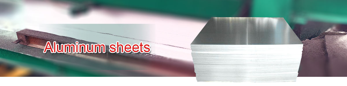
文件大小: 71KB2021-1-29 3003 Aluminum Sheet. Features. ♦ Alloy:3003 ♦ Temper: H14, H16, H18, H22, H24, H26, O ♦ Thickness(mm):0.25-10 ♦ Width(mm):800-2200 ♦ This series aluminum sheet is anticorrosive and
wafer for light cover, cookware aluminium price per kilo 3003 thickness 60mm aluminum wafer. $2,800.00 / Ton. 1 Ton (Min. Order) CN Shandong Hengxin Aluminum Co., Ltd. 1 YRS. Contact
Particle wafers - Particle grade wafers typically refer to 300 mm wafers and have a minimal amount of contaminants, or particles. Particles are measured at various sizes, 0.09 um, 0.12 um, 0.16 um. 0.20
The Si wafer industry has extremely well defined SEMI specifications, and a general outline as to how to properly locate these specifications is given here. Specifications for thin wafers, Double Side Polished
Standard Silicon Wafer Sizes • Minimum thickness is that usually needed for standard processing. • Weight is that of a single wafer at this thickness. diameter min. thickness no. in std. cassette wafer
desired wafer thickness. Several wafers at a time are lapped in between two counter-rotating pads by a slurry consisting of e.g. Al 2 O 3 or SiC abrasive grains with a defi ned size distribution. Etching
Silicon wafers are available in various diameters up to 25 '' 'and can be offered in sizes 4 inch, 6 inch and 12 inch. The thickness of the wafer ranges from 775 "'for a 12-inch wafer to 1.5"' '' for a 6-inch wafer
The common aluminum sheet metal thickness on the market is usually in mm or inches. The usage of aluminum gauge thickness originated in North America. The larger the value, the smaller the actual
Metal Layer Thickness Measurement by Eddy Current Testing. ... (10 mm x 10 mm) or wafer level up to substrate widths of 3,300 mm. Depending on customers requirements (thin film quality, machine
US8220646B2 US13/232,676 US201113232676A US8220646B2 US 8220646 B2 US8220646 B2 US 8220646B2 US 201113232676 A US201113232676 A US 201113232676A US 8220646 B2
Jun 19, 2020 In this example, the thickness is 15.5 cubic cm / 96.774 square cm = 0.16 cm or 1.6 mm. Which side of aluminum foil is toxic? Since aluminum foil has a shiny side and a dull side, many
Specialty Silicon Wafer Products and materials. NOVA is a one stop shop and has been providing the best specialty wafer products for years. We offer products such as: Sapphire Substrates. Synthetic
2021-1-29 3003 Aluminum Sheet. Features. ♦ Alloy:3003 ♦ Temper: H14, H16, H18, H22, H24, H26, O ♦ Thickness(mm):0.25-10 ♦ Width(mm):800-2200 ♦ This series aluminum sheet is anticorrosive and
Particle wafers - Particle grade wafers typically refer to 300 mm wafers and have a minimal amount of contaminants, or particles. Particles are measured at various sizes, 0.09 um, 0.12 um, 0.16 um. 0.20
Wafer size Typical thickness Year introduced Weight per wafer 100 mm2 (10 mm) Die per wafer 1-inch (25 mm) 1960 2-inch (51 mm) 275 μm: 1969 9 3-inch (76 mm) 375 μm 1972 29 4-inch (100 mm) 525
The Si wafer industry has extremely well defined SEMI specifications, and a general outline as to how to properly locate these specifications is given here. Specifications for thin wafers, Double Side Polished
Metal Layer Thickness Measurement by Eddy Current Testing. ... (10 mm x 10 mm) or wafer level up to substrate widths of 3,300 mm. Depending on customers requirements (thin film quality, machine
Presently, a typical thickness of the silicon wafer used by the solar cell industries is about 280/spl sim/330 /spl mu/m. The industry trend is to use thinner wafers to reduce the cost of solar cells. The
Specialty Silicon Wafer Products and materials. NOVA is a one stop shop and has been providing the best specialty wafer products for years. We offer products such as: Sapphire Substrates. Synthetic
Wafer handling options Wafer size: 150/200/300 mm Wafer thickness: 0.3 - 1.5 mm Materials: Si, GaN on Si, glass, Ceramic Warpage Wafer table flow and burl pitch Alignment options Alignment through
May 16, 2014 The wafer calculator then calculates (i) the area and volume of the wafer, (ii) the mass of the wafer, and (iii) the output power and power per gram. Disclaimer. Neither PV Lighthouse nor any
Description: is applicable to wafers 50 mm or larger in diameter, and 100 µm (0.004 in.) approximately and larger in thickness, independent of thickness variation and surface finish, and of wafer shape.
300mm and is about 1 mm thick. 50mm in Wafer – scale: wafer level (~300mm / 12 inch) The wafers are polished until they have flawless, mirror-smooth surfaces. Intel buys manufacturing-ready wafers from
Wafer-level chip-scale package (fan-in WLP and fan-out WLP) Rev. 8 — 10 July 2018 Application note Document information Information Content ... PCB stencil aperture diameter (mm) / thickness (µm)
2021-1-29 3003 Aluminum Sheet. Features. ♦ Alloy:3003 ♦ Temper: H14, H16, H18, H22, H24, H26, O ♦ Thickness(mm):0.25-10 ♦ Width(mm):800-2200 ♦ This series aluminum sheet is anticorrosive and
Wafer size Typical thickness Year introduced Weight per wafer 100 mm2 (10 mm) Die per wafer 1-inch (25 mm) 1960 2-inch (51 mm) 275 μm: 1969 9 3-inch (76 mm) 375 μm 1972 29 4-inch (100 mm) 525
Metal Layer Thickness Measurement by Eddy Current Testing. ... (10 mm x 10 mm) or wafer level up to substrate widths of 3,300 mm. Depending on customers requirements (thin film quality, machine
Apr 26, 2019 Aluminum Film on Silicon Wafer, Al: 300 nm, Si (100) P-type R:1-20 ohm.cm. Found in 1990, Xiamen Powerway Advanced Material Co., Ltd (PAM-XIAMEN) is a leading manufacturer of
Metal thickness measurement. Technology Aluminum Steel ... reflectCONTROL deflectometry systems are used to detect the flatness or planarity of 150 mm wafers. These measure the flatness with only
Wafer handling options Wafer size: 150/200/300 mm Wafer thickness: 0.3 - 1.5 mm Materials: Si, GaN on Si, glass, Ceramic Warpage Wafer table flow and burl pitch Alignment options Alignment through
May 16, 2014 The wafer calculator then calculates (i) the area and volume of the wafer, (ii) the mass of the wafer, and (iii) the output power and power per gram. Disclaimer. Neither PV Lighthouse nor any
GAUGE TO THICKNESS CHART Gauge Stainless Galvanized Sheet Steel Aluminum Fraction inches (mm) inches (mm) inches (mm) inches (mm) 30 0.0125 (0.33) 0.0157 (0.40) 0.0120 (0.30) 0.0100 (0.25)
The most widely used aluminum, 6061 is fabricated into everything from pipe fittings and containers to automotive and aerospace parts. It is strong and corrosion resistant, plus it's easy to machine and
Description: Multi-tool functionality including wafer thickness, shape, global and site flatness Measures up to 8,700 data points per wafer Up to 40 sort classes available Optional resistivity and type
Aug 01, 2021 Fig. 1 illustrates the regime of applied anodizing voltage during the anodization of 200 mm Al wafers at 60 V. Fig. 1b demonstrates the response current density (i) versus anodizing time (t)
Polished Single-Crystal Silicon, Prime Wafers (all numbers nominal) Wafer Specification Table Diameter 100 mm 4-inch 150 mm 6-inch Thickness 525 µm 20.5 mils 675 µm 26.3 mils Primary Flat Length
Diameter 50 To 240mm Thickness 2 To 6mm 3003 Aluminum Wafer 3003 Aluminum Wafer Aluminum Plate Metal Stamping Can Be Customized , Find Complete Details about Diameter 50 To
Aluminum (20-1200 nm) Titanium (20-150 nm) Titanium nitride (20-150 nm) Chromium (20-300 nm) Gold (20-300 nm) Note: thickness ranges may be extended to meet specific needs. Platinum and